![]()
Search Market Research Report
Copper Sputtering Target Market Size, Share Global Analysis Report, 2022 – 2028

Copper Sputtering Target Market Size, Share, Growth Analysis Report By Type (Low Purity Copper Sputtering Target, High Purity Copper Sputtering Target, and Ultra High Purity Copper Sputtering Target), By Application (Semiconductors, Solar Cell, LCD Displays, and Others), and By Region - Global and Regional Industry Insights, Overview, Comprehensive Analysis, Trends, Statistical Research, Market Intelligence, Historical Data and Forecast 2022 – 2028
Industry Insights
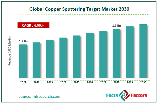
[228+ Pages Report] According to the report published by Facts Factors, the global Copper Sputtering Target market size was worth around USD 1.2 billion in 2021 and is predicted to grow to around USD 1.9 billion by 2028 with a compound annual growth rate (CAGR) of roughly 6.5% between 2022 and 2028. The report analyzes the global Copper Sputtering Target market’s drivers, restraints/challenges, and the effect they have on the demands during the projection period. In addition, the report explores emerging opportunities in the Copper Sputtering Target market.
 Market Overview
Sputtering is a technique that enables the thin film deposition of a metallic or oxide material with ultra-high purity on another solid substance. The development of copper sputtering targets with low electric resistance for the component, capable of high-speed computer operation, is underway. Additionally, the copper sputtering target has an average grain size of about 30 m and 17% of un- homogeneity deposition through an annealing temperature of 0.4 Tm to achieve the deposited thin film uniformity. The gases that are employed in the copper sputtering target process are neon, krypton, xenon, and argon. Copper sputtering targets are reproducible and can be mounted up from R&D projects to production groups involving large to medium substrate regions for efficient energy projected to target mass.
Key Insights
- As per the analysis shared by our research analyst, the global Copper Sputtering Target market is estimated to grow annually at a CAGR of around 6.5% over the forecast period (2022-2028).
- In terms of revenue, the global Copper Sputtering Target market size was valued at around USD 1.2 billion in 2021 and is projected to reach USD 1.9 billion, by 2028. Due to a variety of driving factors, the market is predicted to rise at a significant rate.
- Based on type, the high-purity copper sputtering target segment is growing at the highest CAGR during the forecast period.
- Based on application, the semiconductors segment was dominated in 2021.
- Based on region, North America is projected to dominate the market during the forecast period.
Covid-19 Impact
The COVID-19 pandemic significantly impacted various industries such as oil & gas, manufacturing, retail, and others owing to the strict lockdown imposed by the government across the globe. Moreover, the disruption in the supply chain of the product and services limits the market expansion. Similarly, the copper sputtering target market was negatively impacted by the COVID-19 pandemic due to various factors such as unavailability of raw materials, revenue fall of the semiconductor industry, and others. The semiconductors sector is significantly impacted by COVID-19 on both the supply and demand sides. Semiconductor foundries were forced to cease operations as a result of a short-term imbalance in demand from the consumer electronics industry. The supply chain was also affected, which had an immediate effect on lead times, backlog commitments, projections, costs, and workforce management. For instance, according to secondary analysis, the COVID outbreak will decrease the growth of the semiconductor industry by 0.8%-0.10% in 2020, from 12.5% in 2019. Thus, the COVID-19 pandemic negatively impacted the growth of the copper sputtering target market to a certain extent.
Growth Drivers
- Increasing application of copper sputtering target for semiconductor chip to drive the market growth
The increasing application of copper sputtering targets for semiconductor chips is expected to drive global copper sputtering target market growth during the forecast period. The sputtering target is used for the fabrication of the barrier layer and the packaging metal wiring layer. In the wafer manufacturing process, the target material is mainly used to make the wafer conductive layer, barrier layer, and metal grid. In the chip packaging process, the sputtering target material is used to generate the metal layer under the bump, wiring layer, and other metal materials. Although the amount of target materials used in wafer manufacturing and chip packaging is small, according to SEMI statistics, the cost of target materials in the wafer manufacturing and packaging process accounts for about 3%. However, the quality of sputtering target materials directly affects the uniformity and performance of the conductive layer and barrier layer, and further affects chip transmission speed and stability, so sputtering target materials are the core raw materials for semiconductor production one of the materials. Thus, the increasing application of copper sputtering targets for semiconductor chips is expected to drive market growth.
Restraints
- Difficulty in putting uniformly targets of complex structures hamper the market growth
One of the biggest challenges for the global copper sputtering market is the inability to consistently place targets with complicated geometries and the low deposition rate for some materials in the sputtering target technology. Furthermore, it is anticipated that these issues will be resolved shortly thanks to technological advancements and innovations made by both established and up-and-coming manufacturers in the copper sputtering target market.
Opportunities
- Advancements in semiconductors for consumer electronics provide a lucrative opportunity for the market expansion
The advancements in semiconductors for consumer electronics such as smartphones, tablets, and computers across the globe are expected to provide an attractive opportunity for global copper sputtering target market expansion during the forecast period. For instance, in May 2021, IBM revealed a breakthrough in semiconductor design and manufacturing with the introduction of the first chip in the world to use 2 nm nanosheet technology. Everything from computing to appliances to communications systems, transportation systems, and essential infrastructure depends on semiconductors. Demand for increased chip performance and energy efficiency continues to rise, especially in the era of hybrid cloud, AI, and the Internet of Things. IBM's new 2 nm chip technology helps advance the state-of-the-art in the semiconductor industry, addressing this growing demand. It is projected to achieve 45% higher performance, or 75 % lower energy use, than the present most advanced 7 nm node chips. Thus, these types of development in the market provide a lucrative opportunity for market expansion.
Segmentation Analysis
The global copper sputtering target market is segmented based on type, application, and region
Based on the type, the global market is bifurcated into low purity copper sputtering target, high purity copper sputtering target, and ultra-high purity copper sputtering target. The high-purity copper sputtering target is expected to grow at the highest CAGR during the forecast period. The highest purity can reach 99.9999%. The significant benefits are that the films possess an outstanding level of electrical conductivity and minimized particle formation during the PVD process. However, the ultra-high purity copper sputtering grew at a significant rate during the forecast period. Ultra-high purity copper sputtering target is made of 99.999% or more pure copper. It is the highest grade of copper sputtering target and has the most demanding requirements in terms of quality and performance. Ultra-high purity copper sputtering target is mainly used in semiconductor applications, such as integrated circuits (ICs), photo volts, transistors, and other electronic components.
Based on the application, the global copper sputtering target market is segmented into semiconductors, solar cells, LCD displays, and others. The semiconductor segment was dominated in 2021 and is expected to show its dominance during the forecast period. In semiconductor devices, copper is frequently employed as a sputtering target due to its high conductivity and accessibility in pure form. Due to shrinking transistor size and rising demand for metal-insulator-metal capacitors, which are needed to power mobile devices, their use has increased over time. However, copper's reactivity with oxygen and other atmospheric elements when employed in semiconductor devices might shorten the device's lifetime. So, efforts are being made to identify novel defenses against the air deterioration of the copper.
Recent Developments:
- In March 2022, JX Nippon Mining & Metals Corporation decided to acquire approximately 260,000 m2 of land in Arizona, USA, to reinforce its business producing sputtering targets for semiconductors and develop new business in the US.
Report Scope
Report Attribute |
Details |
Market Size in 2021 |
USD 1.2 Billion |
Projected Market Size in 2028 |
USD 1.9 Billion |
CAGR Growth Rate |
6.5% CAGR |
Base Year |
2021 |
Forecast Years |
2022-2028 |
Key Market Players |
American Elements, JX Nippon Mining & Metals Corporation, Sumitomo Metal Mining Co. Ltd., Honeywell International Inc., Praxair Technology Inc., Vital Materials Co. Limited, Alfa Aesar, Thermo Fisher Scientific, Plansee SE, Mitsubishi Materials Corporation, VEM, and others. |
Key Segment |
By Type, Application, and Region |
Major Regions Covered |
North America, Europe, Asia Pacific, Latin America, and the Middle East &, Africa |
Purchase Options |
Request customized purchase options to meet your research needs. Explore purchase options |
Regional Analysis
- North America is expected to dominate the market during the forecast period
North America is anticipated to hold the major proportion of the worldwide copper sputtering target market, followed by Asia-Pacific. Additionally, this is primarily caused by the rise in semiconductor use as well as the presence of both established and up-and-coming firms that offer copper sputtering targets. Additionally, during the forecast period, the Asia-Pacific market is anticipated to grow at the highest rate. It is anticipated that the regional copper sputtering target market will grow due to the growing demand for semiconductors and electronic devices in the semiconductor and electronics industry. Additionally, the significant economies within the region, including China, Japan, and India, are largely responsible for the advancement prospects for the copper sputtering target market. According to estimates, China is the main nation boosting the region's copper sputtering target market.
Competitive Analysis
- American Elements
- JX Nippon Mining & Metals Corporation
- Sumitomo Metal Mining Co. Ltd.
- Honeywell International Inc.
- Praxair Technology Inc.
- Vital Materials Co. Limited
- Alfa Aesar
- Thermo Fisher Scientific
- Plansee SE
- Mitsubishi Materials Corporation
- VEM.
The global copper sputtering target market is segmented as follows:
By Type
- Low Purity Copper Sputtering Target
- High Purity Copper Sputtering Target
- Ultra-High Purity Copper Sputtering Target
By Application
- Semiconductors
- Solar Cell
- LCD Displays
- Others
By Regional Segment Analysis
- North America
- The U.S.
- Canada
- Mexico
- Europe
- France
- The UK
- Spain
- Germany
- Italy
- Nordic Countries
- Denmark
- Sweden
- Norway
- Benelux Union
- Belgium
- The Netherlands
- Luxembourg
- Rest of Europe
- Asia Pacific
- China
- Japan
- India
- Australia
- South Korea
- Southeast Asia
- Indonesia
- Thailand
- Malaysia
- Singapore
- Rest of Southeast Asia
- Rest of Asia Pacific
- The Middle East & Africa
- Saudi Arabia
- UAE
- Egypt
- South Africa
- Rest of the Middle East & Africa
- Latin America
- Brazil
- Argentina
- Rest of Latin America
Industry Major Market Players
- American Elements
- JX Nippon Mining & Metals Corporation
- Sumitomo Metal Mining Co. Ltd.
- Honeywell International Inc.
- Praxair Technology Inc.
- Vital Materials Co. Limited
- Alfa Aesar
- Thermo Fisher Scientific
- Plansee SE
- Mitsubishi Materials Corporation
- VEM.


Copyright © 2025 - 2026, All Rights Reserved, Facts and Factors